Cmos Technology is Used in Developing
Margins should be set at no less than 1. Supplemental Turabian Style Guidelines.
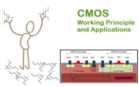
Cmos Technology Working Principle Characteristics Its Applications
The high resolution low cost radar sensor will generate real-time 3D location and velocity map of cars surrounding objects enabling a mass market of safer cars and even auto-driver that will massively disrupt the transportation industry with new.
. Savvas Chamberlain was a pioneer in developing both technologies. In the imaging and sensing field Sony has a great selection of cutting-edge products such as intelligent vision sensors with AI processing functionality ToF image sensors that can be used even for ARMR and automotive image sensors critical to realizing autonomous driving. Check out our series on charge-coupled device CCD image sensors.
The complementary of the Commodore Semiconductor Group CSG or Metal Oxide Semiconductor MOS is called as CMOS technologyThis technology is used in developing the microprocessors microcontrollers digital logic circuits and many other integrated circuitsIt facilitates low- power dissipation and high-packing density with very less noise margin. They are however still used in medium format backs where the benefits of CMOS technology are not as necessary. Only a life lived for others is a life worthwhile The rise of the Genuinfluencers is changing cause marketingfor the better.
RFISee is developing the worlds first 4D imaging-radar-on-1-chip providing the next generation ears and eyes for autonomous vehicles. CCD became dominant primarily because they gave far superior images with the fabrication technology available. Subheadings should be used for longer papers.
During the pandemic social media influencers shifted gears to focus more on highlighting imperfections. Long seen as an inferior competitor to the CCD CMOS sensors have progressed to match or better the CCD standard. Transistors are the active components of integrated circuits or microchips which often contain billions of these minuscule devices etched into their shiny surfaces.
Deeply embedded in almost everything electronic transistors have become the nerve cells of the. Looking ahead Sonys Semiconductor Solutions Group a separate unit from its camera division is developing a next-generation Stacked CMOS Opens in a new window chip that repositions onboard. CMOS recommends you devise your own format but use consistency as your guide.
This information appears in The Chicago Manual of Style section 14103. You can start with the structure and functionality of CCDs. With more functionality built on-chip than CCDs CMOS sensors are able to work more efficiently and.
The unique technologies that lie behind these products are all world firsts and include. Typeface should be something readable such as Times New Roman or. Another related technology development is reported to have developed smart phones with an integrated 36 camera to build VR smart phones with a 16-megapixel 360 camera able to shoot 4K videos 19.
CCDs and CMOS imagers were both invented in the late 1960s and 1970s DALSA founder Dr. We need to invest in the right people and technology first something we might not have the budget for 5. Transistor semiconductor device for amplifying controlling and generating electrical signals.
IBM today unveiled a breakthrough in semiconductor design and process with the development of the worlds first chip announced with 2 nanometer nm nanosheet technologySemiconductors play critical roles in everything from computing to appliances to communication devices transportation systems. An active-pixel sensor APS is an image sensor where each pixel sensor unit cell has a photodetector typically a pinned photodiode and one or more active transistors. In this article well take a look at the basics of CMOS image sensors.
In a metaloxidesemiconductor MOS active-pixel sensor MOS field-effect transistors MOSFETs are used as amplifiersThere are different types of APS including the early NMOS APS and the. For CMOS and Turabians recommendations see Headings below. More efficient smaller lighter faster more reliable with their high current densities and.
In notes CMOS prefers the abbreviation of editors as ed or eds and translators as trans In bibliographic entries these abbreviations are not used. X-FAB is the first pure-play foundry to provide comprehensive processing technologies for the wide-bandgap materials silicon carbide SiC and gallium nitride GaNWide-bandgap materials offer unprecedented benefits for high-power or high-frequency applications. Most CMOS photo-detectors are based on the operation of a PN-junction photodiode.
Instead titles are spelled out in full. Although it will take more time to develop but the possibilities to eventually integrate with smart phones for collecting optical information and data seem to be real and. ALBANY NY May 6 2021 PRNewswire -- IBM NYSE.
An Introduction To Cmos Technology Technical Articles
Possibilities And Limitations Of Cmos Technology For The Production Of Various Microelectronic Systems And Devices Springerlink

An Introduction To Cmos Technology Technical Articles
Cmos Technology Working Principle Characteristics Its Applications
No comments for "Cmos Technology is Used in Developing"
Post a Comment